Researchers at Columbia University have made significant strides in the field of quantum technologies by developing a method to enhance nonlinear optical effects at the nanoscale. Led by Jim Schuck, a professor of mechanical engineering, the team has created a novel crystalline device just 3.4 micrometers thick, capable of generating entangled photon pairs, a crucial element for advancing quantum computing.
In a paper published in October 2025 in Nature Photonics, the researchers unveiled an innovative approach that reduces nonlinear platforms to a mere 160 nanometers. This achievement was made possible through the introduction of metasurfaces—artificial geometries etched into ultrathin crystals, granting them enhanced optical properties. Chiara Trovatello, the corresponding author and assistant professor at Politecnico di Milano, stated, “We’ve established a successful recipe to pattern ultrathin crystals at the nanoscale to enhance nonlinearity while maintaining their sub-wavelength thickness.”
The Schuck lab focuses on a specific class of crystals known as transition metal dichalcogenides (TMDs). These materials can be thinned down to atom-thin layers and assembled into customizable stacks. Despite their remarkable nonlinear properties, traditional TMDs were not efficient enough for generating photons at new frequencies compared to conventional nonlinear crystals, which are commonly used in everyday devices like laser pointers. Trovatello emphasized the importance of size in quantum technologies, saying, “To make quantum technologies scalable, we need to shrink the size of our qubit sources.”
Earlier in January 2025, the team published a paper demonstrating how they used a technique called periodic poling to generate photons capable of powering qubits. This involved layering molybdenum disulfide in alternating directions to optimize its optical output, ensuring that light waves remained phase-matched. The recent findings detail a complementary method utilizing metasurfaces with etched patterns.
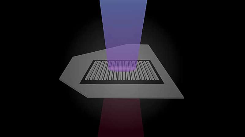
Metasurfaces have the potential to introduce novel optical properties that do not exist in unmodified crystals. By strategically removing sections of atoms, researchers create new periodic geometries, leading to enhanced functionalities. Zhi Hao Peng, a Ph.D. student and the first author of the study, developed a nanofabrication technique that involved etching a series of repeating lines onto a flake of molybdenum disulfide. “Our design enhances the nonlinear effects much more than traditional linear optical optimization techniques,” Peng explained, noting that their metasurface improved second-harmonic generation by nearly 150 times compared to unpatterned samples.
Second-harmonic generation is a process where two photons combine to create a new photon with double the frequency and half the wavelength. With this optimization achieved, the research team is now focusing on reversing the process to split one photon into two entangled photons. Notably, Peng’s method requires fewer steps, making it more efficient and cost-effective than previous approaches.
Schuck remarked on the challenges of working with nonlinear crystals, stating, “These materials can be brittle and have been notoriously difficult to shape and fabricate.” However, Peng’s technique offers a simple solution that allows for increasingly complex patterns using standard cleanroom etching technologies.
Theoretical collaborators, including Andrea Alu from the CUNY Advanced Science Research Center, played a crucial role in determining the metasurface patterns necessary to achieve significant nonlinear responses across ultrathin path lengths. Michele Cortufo, a former postdoctoral researcher with Alu, also contributed to the research. Cortufo noted, “We showed that such nontrivial behavior can be obtained with a remarkably simple modification to the sample.”
This innovative research signifies a leap in the nanoscale optical devices field, with implications for creating compact, integrable platforms for nonlinear optics and light generation. The light generated operates at telecommunications-range wavelengths, making it easily compatible with existing networks and devices.
Schuck expressed optimism about the future applications of this work, stating, “This could be one of the most compact sources of entangled photons at that wavelength range. With our footprint, we can really start to think about fully on-chip quantum photonics.”
As researchers continue to explore the potential of these nanoscale devices, the advancements made at Columbia University promise to reshape the landscape of quantum technologies and photonics. For further details, refer to the study by Zhi Hao Peng et al, titled “3R-stacked transition metal dichalcogenide non-local metasurface for efficient second-harmonic generation,” published in Nature Photonics.


